Semiconductor
Display
Vacuum system
Heating system
Semiconductor
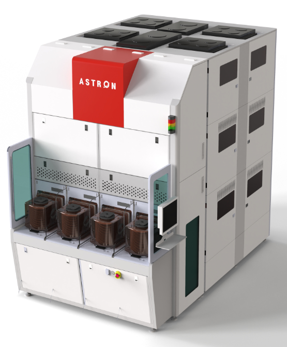
This system rotates a semiconductor wafer one by one and sprays a variety of cleaning solutions in order to remove pollutants on the surface and back of the wafer.

Feature
- Smallest Footprint
– A process chamber has a compact size, so that it can installed in 1F to 4F. It has the smallest footprint in the world.
- Highest Throughput
– The wafer processing throughput per footprint is the highest in the world.
– Wafer transfer system optimization and 4-hand robot for smooth large-capacity process
Specifications
- Chamber quantity : 1 / 2 / 4 / 8 / 12 / 16 / 24
- Process : Cleaning, Etching, Stripping
- Wafer size : 200mm, 300mm (Making a special type of wafer is available.)